
Applied Materials Unveils Advanced Deposition Tools for the Angstrom Era of Chipmaking!
Applied Materials is advancing the future of semiconductor manufacturing with the introduction of two new deposition systems designed to support the transition to angstrom-scale chipmaking. These innovations are aimed at enabling the production of next-generation chips at 2nm-class nodes and beyond, where precision at the atomic level becomes critical to performance, power efficiency, and yield.
As the semiconductor industry moves from FinFET architectures to Gate-All-Around transistors, the complexity of chip fabrication is increasing dramatically. Advanced logic processes can now exceed 500 steps, many of which involve highly controlled deposition of materials across intricate three-dimensional structures. This shift is being driven in large part by the demands of artificial intelligence, where next-generation processors are expected to integrate hundreds of billions of transistors within extremely compact footprints.
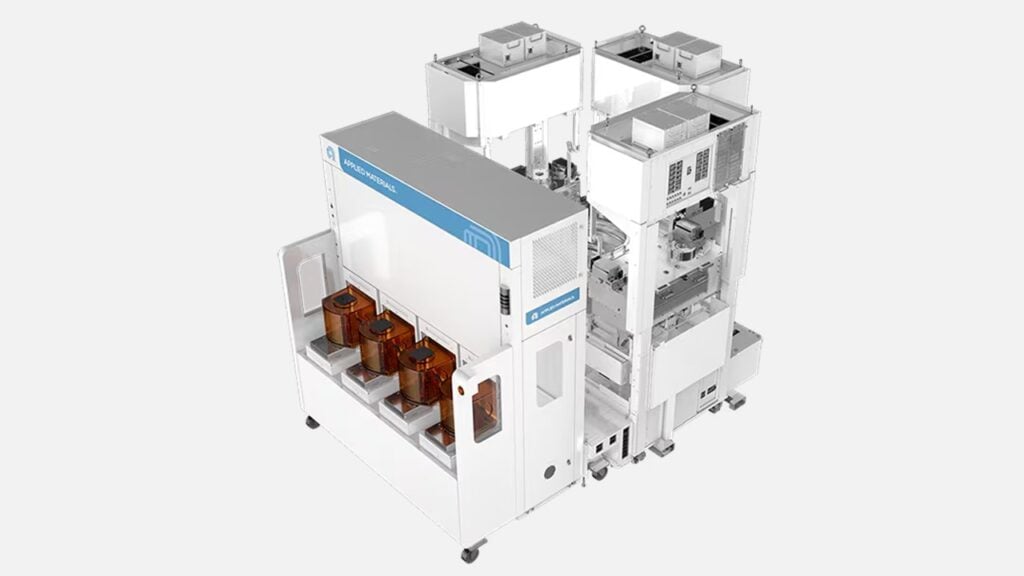
To address these challenges, Applied Materials has introduced its Precision Selective Nitride PECVD system. This platform is designed to deposit silicon nitride films with high selectivity, helping protect shallow trench isolation structures that are essential for maintaining electrical separation between densely packed transistors. By improving isolation integrity, the system contributes to reduced parasitic capacitance and enhanced overall device performance, which are increasingly important as transistor density continues to rise.
The second innovation, the Trillium ALD system, focuses on one of the most critical aspects of advanced transistor design: the formation of metal gate stacks in Gate-All-Around architectures. These structures require ultra-thin, conformal layers to be deposited with extreme precision over complex nanoscale geometries. The Trillium platform enables tighter control over these layers, directly influencing key parameters such as threshold voltage and device variability. At angstrom-scale dimensions, even the smallest inconsistencies can impact chip performance and manufacturing yield, making such precision indispensable.
According to Prabu Raja, President of the Semiconductor Products Group at Applied Materials, the industry is entering a phase of rapid and non-linear change where traditional scaling approaches are no longer sufficient. He emphasized that materials engineering is becoming a defining factor in determining chip performance and power efficiency at advanced nodes. The newly introduced deposition systems are positioned as critical enablers for achieving the transistor-level breakthroughs required by the AI computing roadmap.
Leading foundries and logic manufacturers are already adopting these systems for 2nm-class development, underscoring the growing importance of deposition control and material precision in next-generation chip production. As semiconductor devices continue to shrink, the margin for error narrows significantly, placing greater emphasis on technologies that can deliver consistent, atomic-level accuracy.
Overall, Applied Materials’ latest innovations highlight a broader industry shift where materials science and deposition technology are at the forefront of semiconductor advancement. By addressing key challenges in isolation and gate-stack formation, these new systems provide a practical pathway for managing variability, reducing power consumption, and sustaining performance gains in the angstrom era of chipmaking.